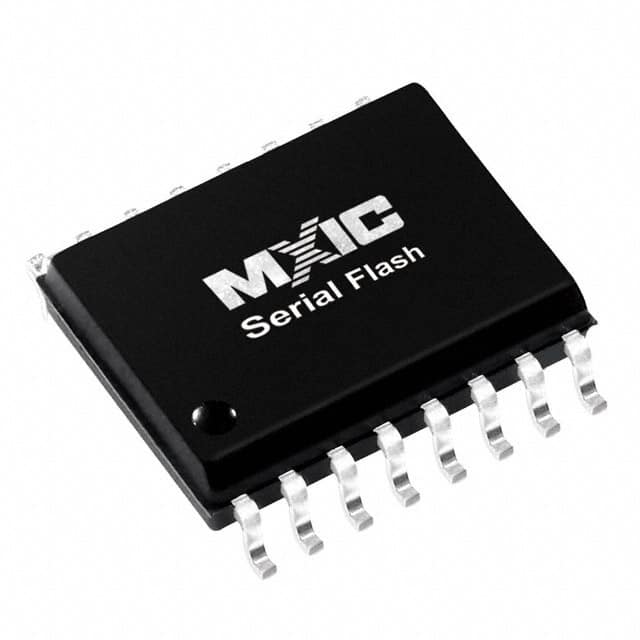
Macronix MX30LF1G08AA-TI

Изображение только для справки, пожалуйста, обратитесь к спецификации продукта
- MX30LF1G08AA-TI
- Macronix
- IC FLASH 1GBIT PARALLEL 48TSOP
- General Memory
- MX30LF1G08AA-TI Лист данных
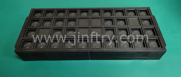
- 48-TFSOP (0.724\", 18.40mm Width)
- Tray
-
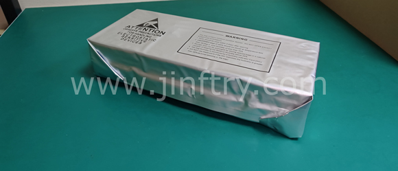
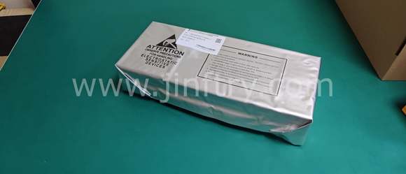
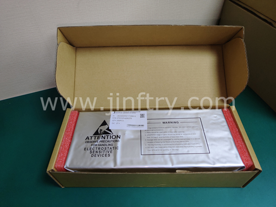
 Lead free / RoHS Compliant
 - 3501
- Запасы спот / разрешенные дилеры / излишки на заводе
- Гарантия качества на 1 год 》
- Нажмите, чтобы узнать цены
Службы доставки:

Способы оплаты:

| Part Number MX30LF1G08AA-TI |
| Category General Memory |
| Manufacturer Macronix |
| Description IC FLASH 1GBIT PARALLEL 48TSOP |
| Package Tray |
| Series MX30LF |
| Voltage - Supply 2.7V ~ 3.6V |
| Operating Temperature -40°C ~ 85°C (TA) |
| Mounting Type Surface Mount |
| Package / Case 48-TFSOP (0.724\", 18.40mm Width) |
| Supplier Device Package 48-TSOP |
| Memory Size 1Gb (128M x 8) |
| Technology FLASH - NAND |
| Memory Type Non-Volatile |
| Clock Frequency - |
| Access Time 30 ns |
| Memory Format FLASH |
| Write Cycle Time - Word, Page 30ns |
| Memory Interface Parallel |
| Package_case 48-TFSOP (0.724\", 18.40mm Width) |
MX30LF1G08AA-TI Гарантии


• Ответьте оперативно
• Гарантированное качество
• Глобальный доступ
• Конкурентоспособная рыночная цена
• Универсальные услуги цепочки поставок
Jinftry, это ваш самый надежный поставщик компонентов, добро пожаловать, чтобы отправить нам запрос, спасибо!
У вас есть вопросы о MX30LF1G08AA-TI ?
Не стесняйтесь связаться с нами:
+86-755-82518276
+8615019224070, annies65, +8615118125813
568248857, 827259012, 316249462
+8615019224070, +8615118118839, +8615118125813
( Электронная почта в первую очередь )
MX30LF1G08AA-TI сопутствующие товары


Комментарии
Macronix

MX30LF4G18AC-TI
IC FLASH 4GBIT PARALLEL 48TSOP

MX25L2006EZNI-12G
IC FLASH 4GBIT PARALLEL 48TSOP

MX25U8035EZUI-10G
IC FLASH 4GBIT PARALLEL 48TSOP
MX25L3206EMI-12G
IC FLASH 4GBIT PARALLEL 48TSOP

MX25L8006EZUI-12G
IC FLASH 4GBIT PARALLEL 48TSOP

MX25V8006EZNI-13G
IC FLASH 4GBIT PARALLEL 48TSOP

MX29F400CTMI-70G
IC FLASH 4GBIT PARALLEL 48TSOP

MX29GL640EBTI-70G
IC FLASH 4GBIT PARALLEL 48TSOP
battery charger
Battery charger according to the design circuit operating frequency to divide, can be divided into power frequency machine and high frequency machine. The power frequency machine is designed based on the traditional analog circuit principle, the internal power devices (such as transformers, inductors, capacitors, etc.) are larger, and there is generally less noise when the load is larger, but the model has strong resistance performance in the harsh grid environmental conditions, and the reliabil
What is the structure and function of PCB?
PCB (Printed Circuit Board) is one of the basic components in modern electronic equipment. It provides a platform to support and connect electronic components.
The internal structure of PCB is composed of multi-layer circuit board, conductive layer, insulating layer, pad, circuit layer, circuit spacing, circuit spacing, via holes, silk screen layer and solder mask layer. These components cooperate with each other to form a complete circuit board, providing reliable electrical connection and pro
How a programmable gate array (FPGA) works, its architecture, and how to program it
How a programmable gate array (FPGA) works, its architecture, and how to program it
Programmable Gate Array (FPGA, Field-Programmable Gate Array) is an integrated circuit that designers can program according to their needs after purchase. It includes a series of logic blocks and reconfigurable interconnections that allow designers to customize specific logic functions, data paths, or other specific circuit functions at the hardware level.
ADI AD5627R/AD5647R/AD5667 series have 12C compatible data transmission capability
AD5667RBRMZ, AD5667BCPZ-REEL7, AD5667RBCPZ-R2, AD5676BRUZ, AD5693RARMZ, AD623ARZ-RL, AD5592RBCPZ-1-RL7.The ADI models briefly described above are in stock at jinftry.com, welcome to consult