Maxim Integrated DS1330BL-70IND

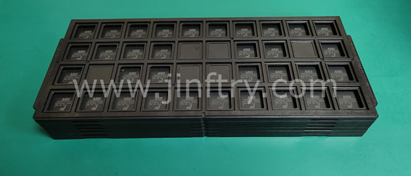
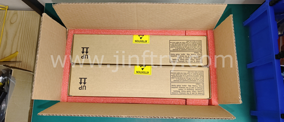
Изображение только для справки, пожалуйста, обратитесь к спецификации продукта
- DS1330BL-70IND
- Maxim Integrated
- IC NVSRAM 256KBIT PARALLEL 34LPM
- General Memory
- DS1330BL-70IND Лист данных
- 34-LPM
- Tube
-
 Lead free / RoHS Compliant
 - 2483
- Запасы спот / разрешенные дилеры / излишки на заводе
- Гарантия качества на 1 год 》
- Нажмите, чтобы узнать цены
Службы доставки:

Способы оплаты:

| Part Number DS1330BL-70IND |
| Category General Memory |
| Manufacturer Maxim Integrated |
| Description IC NVSRAM 256KBIT PARALLEL 34LPM |
| Package Tube |
| Series - |
| Voltage - Supply 4.75V ~ 5.25V |
| Operating Temperature -40°C ~ 85°C (TA) |
| Mounting Type Surface Mount |
| Package / Case 34-LPM |
| Supplier Device Package 34-LPM |
| Memory Size 256Kb (32K x 8) |
| Technology NVSRAM (Non-Volatile SRAM) |
| Memory Type Non-Volatile |
| Clock Frequency - |
| Access Time 70 ns |
| Memory Format NVSRAM |
| Write Cycle Time - Word, Page 70ns |
| Memory Interface Parallel |
| Package_case 34-LPM |
DS1330BL-70IND Гарантии


• Ответьте оперативно
• Гарантированное качество
• Глобальный доступ
• Конкурентоспособная рыночная цена
• Универсальные услуги цепочки поставок
Jinftry, это ваш самый надежный поставщик компонентов, добро пожаловать, чтобы отправить нам запрос, спасибо!
У вас есть вопросы о DS1330BL-70IND ?
Не стесняйтесь связаться с нами:
+86-755-82518276
+8615019224070, annies65, +8615118125813
568248857, 827259012, 316249462
+8615019224070, +8615118118839, +8615118125813
( Электронная почта в первую очередь )
DS1330BL-70IND сопутствующие товары


Комментарии
Maxim Integrated

DS1245AB-100
IC NVSRAM 1MBIT PARALLEL 32EDIP
DS1345ABP-70IND
IC NVSRAM 1MBIT PARALLEL 32EDIP
DS1345YP-70IND
IC NVSRAM 1MBIT PARALLEL 32EDIP

DS1330BL-70
IC NVSRAM 1MBIT PARALLEL 32EDIP

DS1330YL-70
IC NVSRAM 1MBIT PARALLEL 32EDIP

DS1345WP-100IND
IC NVSRAM 1MBIT PARALLEL 32EDIP

DS1330YL-100
IC NVSRAM 1MBIT PARALLEL 32EDIP

DS1330BL-100
IC NVSRAM 1MBIT PARALLEL 32EDIP
What Are Clock ICs and How Do They Work in Electronic devices?
What Are Clock ICs and How Do They Work in Electronic devices?Clock Integrated Circuits (ICs) are vital components in timing electronic devices that regulate the timing and synchronization of various operations within a system. They generate precise timing signals necessary for the proper functioning of digital circuits. Clock ICs come in various types, each serving specific purposes in electronic systems.
What is the difference between FPGA and GPU
Difference Between FPGA and GPU
FPGA (field programmable gate array) and GPU (graphics processing unit) are two common hardware accelerators used to increase computing and processing speed. Although they overlap in many ways, there are many differences in architecture, design, and application. In this article, we will explore the differences between FPGAs and GPUs in detail.
74LS74 Double D Flip-Flop Characteristics Pin Data Sheet Application - Can Replace Introduction
74LS74 Pinout
74LS74 CAD Model
74LS74 Features
74LS74 Application
74LS74 Equivalent
What is 74LS74?
How to Use 74LS74
74LS74 Connection Diagram
74LS74 Package
74LS74 Manufacturer
Specifications
Parts with Similar Specs
How a programmable gate array (FPGA) works, its architecture, and how to program it
How a programmable gate array (FPGA) works, its architecture, and how to program it
Programmable Gate Array (FPGA, Field-Programmable Gate Array) is an integrated circuit that designers can program according to their needs after purchase. It includes a series of logic blocks and reconfigurable interconnections that allow designers to customize specific logic functions, data paths, or other specific circuit functions at the hardware level.