Renesas Electronics America Inc 9DBV0731AKILF

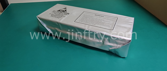
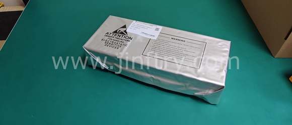
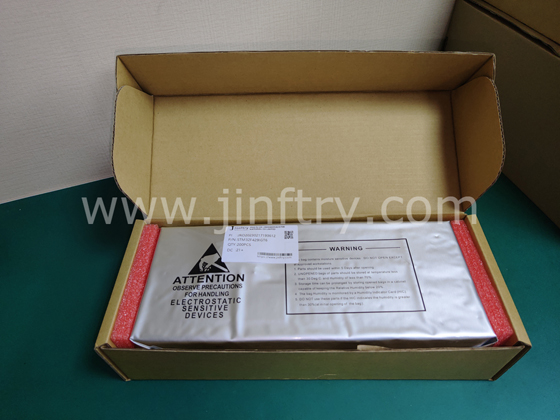
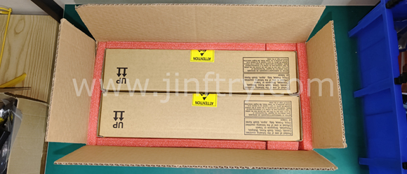
Изображение только для справки, пожалуйста, обратитесь к спецификации продукта
- 9DBV0731AKILF
- Renesas Electronics America Inc
- VFQFPN 5.00X5.00X0.90 MM, 0.40MM
- Clock/Timing - Application Specific
- 9DBV0731AKILF Лист данных
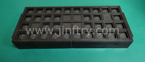
- 40-VFQFN Exposed Pad
- Tray
-
 Lead free / RoHS Compliant
 - 16814
- Запасы спот / разрешенные дилеры / излишки на заводе
- Гарантия качества на 1 год 》
- Нажмите, чтобы узнать цены
Службы доставки:

Способы оплаты:

| Part Number 9DBV0731AKILF |
| Category Clock/Timing - Application Specific |
| Manufacturer Renesas Electronics America Inc |
| Description VFQFPN 5.00X5.00X0.90 MM, 0.40MM |
| Package Tray |
| Series - |
| Voltage - Supply 1.7V ~ 1.9V |
| Operating Temperature -40°C ~ 85°C (TA) |
| Mounting Type Surface Mount |
| Package / Case 40-VFQFN Exposed Pad |
| Supplier Device Package 40-VFQFPN (5x5) |
| Output LP-HCSL |
| Frequency - Max 200MHz |
| Number of Circuits 1 |
| Input HCSL |
| PLL Yes |
| Main Purpose Ethernet, PCI Express (PCIe) |
| Ratio - Input:Output 1:7 |
| Differential - Input:Output Yes/Yes |
| Package_case 40-VFQFN Exposed Pad |
9DBV0731AKILF Гарантии


• Ответьте оперативно
• Гарантированное качество
• Глобальный доступ
• Конкурентоспособная рыночная цена
• Универсальные услуги цепочки поставок
Jinftry, это ваш самый надежный поставщик компонентов, добро пожаловать, чтобы отправить нам запрос, спасибо!
У вас есть вопросы о 9DBV0731AKILF ?
Не стесняйтесь связаться с нами:
+86-755-82518276
+8615019224070, annies65, +8615118125813
568248857, 827259012, 316249462
+8615019224070, +8615118118839, +8615118125813
( Электронная почта в первую очередь )
9DBV0731AKILF сопутствующие товары


Комментарии
Renesas Electronics America Inc

9DMU0141AKILF
IC MUX PCIE 2:1 1.5V 16VFQFPN
CSPUA877ANLG
IC MUX PCIE 2:1 1.5V 16VFQFPN
9FGV0831CKLF
IC MUX PCIE 2:1 1.5V 16VFQFPN

9DBU0831AKLF
IC MUX PCIE 2:1 1.5V 16VFQFPN

9DBU0931AKLF
IC MUX PCIE 2:1 1.5V 16VFQFPN

9DBU0941AKLF
IC MUX PCIE 2:1 1.5V 16VFQFPN

9FGL06P1B000KILFT
IC MUX PCIE 2:1 1.5V 16VFQFPN

9FGU0641AKILFT
IC MUX PCIE 2:1 1.5V 16VFQFPN
What is Logic IC?
What is Logic IC?
What are the main functions of logic IC?
Type of standard Logic ICs
What are the advantages of using logic IC?
Equipment in Which Logic ICs are used?
What is the difference between FPGA and GPU
Difference Between FPGA and GPU
FPGA (field programmable gate array) and GPU (graphics processing unit) are two common hardware accelerators used to increase computing and processing speed. Although they overlap in many ways, there are many differences in architecture, design, and application. In this article, we will explore the differences between FPGAs and GPUs in detail.
What is a programmable logic IC?
What is a programmable logic IC?
A programmable logic device (PLD) is a special type of electronic component used in electronic systems. Unlike logic gates, which have fixed functionality, PLDs are manufactured with undefined functionality. They are highly flexible electronic components that can be programmed to be configured to perform a variety of logic functions.
Here's a closer look at some of the main types:
PLD (Programmable Logic Device): This is a basic form of programmable logic
How a programmable gate array (FPGA) works, its architecture, and how to program it
How a programmable gate array (FPGA) works, its architecture, and how to program it
Programmable Gate Array (FPGA, Field-Programmable Gate Array) is an integrated circuit that designers can program according to their needs after purchase. It includes a series of logic blocks and reconfigurable interconnections that allow designers to customize specific logic functions, data paths, or other specific circuit functions at the hardware level.