Altera 5SGXMA5H2F35I2LN

Изображение только для справки, пожалуйста, обратитесь к спецификации продукта
- 5SGXMA5H2F35I2LN
- Altera
- IC FPGA 552 I/O 1152FBGA
- Embedded - FPGAs (Field Programmable Gate Array)
- 5SGXMA5H2F35I2LN Лист данных
- 1152-BBGA, FCBGA
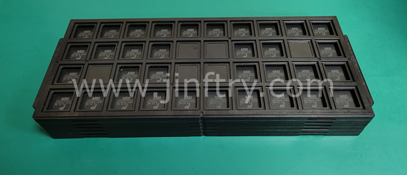
- Tray
-
 Lead free / RoHS Compliant
 - 3393
- Запасы спот / разрешенные дилеры / излишки на заводе
- Гарантия качества на 1 год 》
- Нажмите, чтобы узнать цены
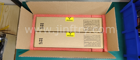
Службы доставки:

Способы оплаты:

| Part Number 5SGXMA5H2F35I2LN |
| Category Embedded - FPGAs (Field Programmable Gate Array) |
| Manufacturer Altera |
| Description IC FPGA 552 I/O 1152FBGA |
| Package Tray |
| Series Stratix® V GX |
| Voltage - Supply 0.82V ~ 0.88V |
| Operating Temperature -40°C ~ 100°C (TJ) |
| Mounting Type Surface Mount |
| Package / Case 1152-BBGA, FCBGA |
| Supplier Device Package 1152-FBGA (35x35) |
| Number of I/O 552 |
| Number of Gates - |
| Number of LABs/CLBs 185000 |
| Number of Logic Elements/Cells 490000 |
| Total RAM Bits 46080000 |
| Package_case 1152-BBGA, FCBGA |


5SGXMA5H2F35I2LN Гарантии


• Ответьте оперативно
• Гарантированное качество
• Глобальный доступ
• Конкурентоспособная рыночная цена
• Универсальные услуги цепочки поставок
Jinftry, это ваш самый надежный поставщик компонентов, добро пожаловать, чтобы отправить нам запрос, спасибо!
У вас есть вопросы о 5SGXMA5H2F35I2LN ?
Не стесняйтесь связаться с нами:
+86-755-82518276
+8615019224070, annies65, +8615118125813
568248857, 827259012, 316249462
+8615019224070, +8615118118839, +8615118125813
( Электронная почта в первую очередь )
5SGXMA5H2F35I2LN сопутствующие товары


Комментарии
Altera

EP2S130F1020I4N
IC FPGA 742 I/O 1020FBGA
10AX115U4F45E3LG
IC FPGA 742 I/O 1020FBGA
5SGXMA9N3F45C4N
IC FPGA 742 I/O 1020FBGA
5SGSMD5K2F40C3
IC FPGA 742 I/O 1020FBGA

5SGXEA4K2F35I2L
IC FPGA 742 I/O 1020FBGA

EP4SGX360KF40C4
IC FPGA 742 I/O 1020FBGA

5SGXEA5K2F35C2L
IC FPGA 742 I/O 1020FBGA

5SGXEA5K2F35I3L
IC FPGA 742 I/O 1020FBGA
What does a power management IC do?
What Are Power Management ICs?
What does a power management IC do?
Classification of Power Management IC
Applications of Power Management IC
How to find a trust supplier of Power Management IC Supplier?
What is the structure and function of PCB?
PCB (Printed Circuit Board) is one of the basic components in modern electronic equipment. It provides a platform to support and connect electronic components.
The internal structure of PCB is composed of multi-layer circuit board, conductive layer, insulating layer, pad, circuit layer, circuit spacing, circuit spacing, via holes, silk screen layer and solder mask layer. These components cooperate with each other to form a complete circuit board, providing reliable electrical connection and pro
NVIDIA A100 80GB PCIe, A100 80GB SXM TENSOR CORE GPU is available in stock
Basic specifications of the NVIDIA A100 (these figures may vary by specific model and configuration):
GPU architecture: Ampere
Number of SMs: 108
Number of CUDA cores: 6912
Number of second-generation RT cores: 108
Number of third-generation Tensor cores: 432
Base Clock Frequency: 1410 MHz
Boost Clock Frequency: 1560 MHz
Memory size: 40GB or 80GB of HBM2
Memory bandwidth: 1555 GB/s (40GB version) or 2039 GB/s (80GB version)
Memory interface width: 5120 bits (40GB version) or 6144 bit
Brief introduction of MSP430G2553 microcontroller
Brief introduction of MSP430G2553 microcontroller
1MSP430G2553 overview
• Low Supply Voltage Range: 1.8V to 3.6V
• Ultra-low power consumption
Run Mode: 230µA at 1MHz and 2.2V
Standby mode: 0.5μA
Off Mode (RAM Retention): 0.1μ
• 5 energy saving modes
• Ultra-fast wake-up from standby mode in less than 1μs
• 16-bit Reduced Instruction Set (RISC) Architecture, 62.5ns Instruction Cycle Time
• Basic clock module configuration
Internal frequency up to 16MHz with four