Altera 5SGXMA3K2F40C2LN

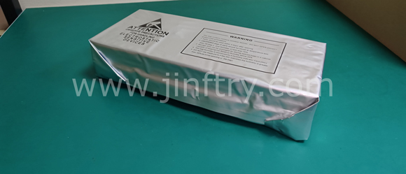
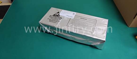
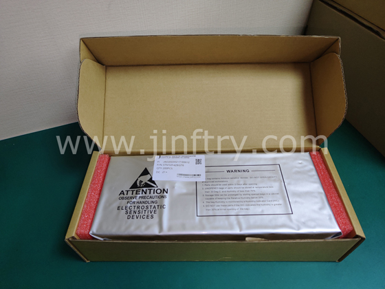
Изображение только для справки, пожалуйста, обратитесь к спецификации продукта
- 5SGXMA3K2F40C2LN
- Altera
- IC FPGA 600 I/O 1517FBGA
- Embedded - FPGAs (Field Programmable Gate Array)
- 5SGXMA3K2F40C2LN Лист данных
- 1517-BBGA, FCBGA
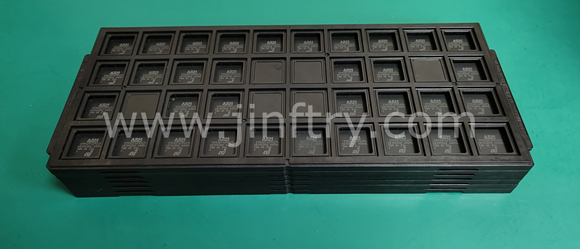
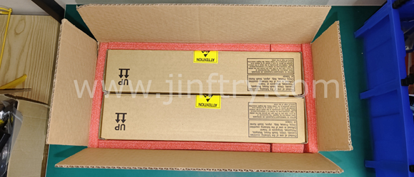
- Tray
-
 Lead free / RoHS Compliant
 - 1975
- Запасы спот / разрешенные дилеры / излишки на заводе
- Гарантия качества на 1 год 》
- Нажмите, чтобы узнать цены
Службы доставки:

Способы оплаты:

| Part Number 5SGXMA3K2F40C2LN |
| Category Embedded - FPGAs (Field Programmable Gate Array) |
| Manufacturer Altera |
| Description IC FPGA 600 I/O 1517FBGA |
| Package Tray |
| Series Stratix® V GX |
| Voltage - Supply 0.82V ~ 0.88V |
| Operating Temperature 0°C ~ 85°C (TJ) |
| Mounting Type Surface Mount |
| Package / Case 1517-BBGA, FCBGA |
| Supplier Device Package 1517-FBGA (40x40) |
| Number of I/O 600 |
| Number of Gates - |
| Number of LABs/CLBs 128300 |
| Number of Logic Elements/Cells 340000 |
| Total RAM Bits 19456000 |
| Package_case 1517-BBGA, FCBGA |
5SGXMA3K2F40C2LN Гарантии


• Ответьте оперативно
• Гарантированное качество
• Глобальный доступ
• Конкурентоспособная рыночная цена
• Универсальные услуги цепочки поставок
Jinftry, это ваш самый надежный поставщик компонентов, добро пожаловать, чтобы отправить нам запрос, спасибо!
У вас есть вопросы о 5SGXMA3K2F40C2LN ?
Не стесняйтесь связаться с нами:
+86-755-82518276
+8615019224070, annies65, +8615118125813
568248857, 827259012, 316249462
+8615019224070, +8615118118839, +8615118125813
( Электронная почта в первую очередь )
5SGXMA3K2F40C2LN сопутствующие товары


Комментарии
Altera

5SGXMA3K1F40I2N
IC FPGA 600 I/O 1517FBGA
5SGXMA3K1F40C2N
IC FPGA 600 I/O 1517FBGA
5SGXMA3K1F40C2LN
IC FPGA 600 I/O 1517FBGA
5SGXMA3K1F40C1N
IC FPGA 600 I/O 1517FBGA

5SGXEB6R3F40C4N
IC FPGA 600 I/O 1517FBGA

5SGXEB6R3F40C4
IC FPGA 600 I/O 1517FBGA

5SGXEB6R3F40C3N
IC FPGA 600 I/O 1517FBGA

5SGXEB6R3F40C3
IC FPGA 600 I/O 1517FBGA
What is the structure and function of PCB?
PCB (Printed Circuit Board) is one of the basic components in modern electronic equipment. It provides a platform to support and connect electronic components.
The internal structure of PCB is composed of multi-layer circuit board, conductive layer, insulating layer, pad, circuit layer, circuit spacing, circuit spacing, via holes, silk screen layer and solder mask layer. These components cooperate with each other to form a complete circuit board, providing reliable electrical connection and pro
FT234XD-R USB datasheet PDF, pin assignments, application areas
FT234XD-R USB datasheet PDF, pin assignments, application areas
FT234XD-R Introduction:
The FT234XD-R provides a bridge from USB to basic UART. This device is ideal for many applications, especially those that do not require complex input/output or a large number of pins, but do require USB functionality. It provides simplified functionality while maintaining the high quality and performance of FTDI's USB 2.0 devices.
How a programmable gate array (FPGA) works, its architecture, and how to program it
How a programmable gate array (FPGA) works, its architecture, and how to program it
Programmable Gate Array (FPGA, Field-Programmable Gate Array) is an integrated circuit that designers can program according to their needs after purchase. It includes a series of logic blocks and reconfigurable interconnections that allow designers to customize specific logic functions, data paths, or other specific circuit functions at the hardware level.
NVIDIA (NVIDIA) provides the following key technical support for artificial intelligence (AI)
1: TDA2x series: This is a System-on-Chip (SoC) for Advanced Driver Assistance Systems (ADAS) with vision processing for environment awareness and multi-camera applications. Such as TDA2003AH, TDA2003AH, TDA20137, TDA20137/1,557, TDA2030V, etc.
2: TDA3x series: This is a more compact ADAS SoC for forward-facing camera and driver monitoring systems, including low-power applications. For example TDA3602/N3,112, TDA3606AT/N1,112, TDA3608TH/N3C,512, TDA3616SF/N1,112 etc.
3:DRA77x "Jacinto