Altera 5SGXEA7K3F40C3

Изображение только для справки, пожалуйста, обратитесь к спецификации продукта
- 5SGXEA7K3F40C3
- Altera
- IC FPGA 696 I/O 1517FBGA
- Embedded - FPGAs (Field Programmable Gate Array)
- 5SGXEA7K3F40C3 Лист данных
- 1517-BBGA, FCBGA
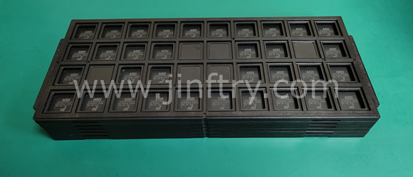
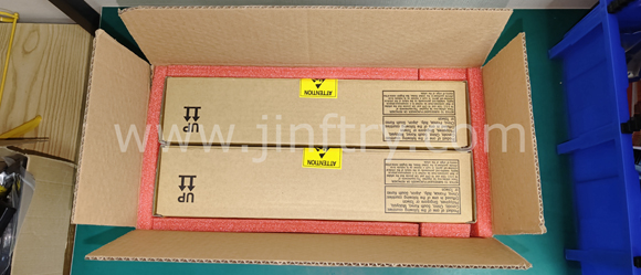
- Tray
-
 Lead free / RoHS Compliant
 - 23328
- Запасы спот / разрешенные дилеры / излишки на заводе
- Гарантия качества на 1 год 》
- Нажмите, чтобы узнать цены
Службы доставки:

Способы оплаты:

| Part Number 5SGXEA7K3F40C3 |
| Category Embedded - FPGAs (Field Programmable Gate Array) |
| Manufacturer Altera |
| Description IC FPGA 696 I/O 1517FBGA |
| Package Tray |
| Series Stratix® V GX |
| Voltage - Supply 0.82V ~ 0.88V |
| Operating Temperature 0°C ~ 85°C (TJ) |
| Mounting Type Surface Mount |
| Package / Case 1517-BBGA, FCBGA |
| Supplier Device Package 1517-FBGA (40x40) |
| Number of I/O 696 |
| Number of Gates - |
| Number of LABs/CLBs 234720 |
| Number of Logic Elements/Cells 622000 |
| Total RAM Bits 51200000 |
| Package_case 1517-BBGA, FCBGA |
5SGXEA7K3F40C3 Гарантии


• Ответьте оперативно
• Гарантированное качество
• Глобальный доступ
• Конкурентоспособная рыночная цена
• Универсальные услуги цепочки поставок
Jinftry, это ваш самый надежный поставщик компонентов, добро пожаловать, чтобы отправить нам запрос, спасибо!
У вас есть вопросы о 5SGXEA7K3F40C3 ?
Не стесняйтесь связаться с нами:
+86-755-82518276
+8615019224070, annies65, +8615118125813
568248857, 827259012, 316249462
+8615019224070, +8615118118839, +8615118125813
( Электронная почта в первую очередь )
5SGXEA7K3F40C3 сопутствующие товары


Комментарии
Altera

5SGXEA7K3F40I4
IC FPGA 696 I/O 1517FBGA
5SGSED8N3F45C4N
IC FPGA 696 I/O 1517FBGA
EP3SL200F1517C4LN
IC FPGA 696 I/O 1517FBGA
5SGXEA4H2F35C1N
IC FPGA 696 I/O 1517FBGA

10AX090H1F34I1SG
IC FPGA 696 I/O 1517FBGA

5SGXEA5K3F40I3L
IC FPGA 696 I/O 1517FBGA

5SGXEA5K2F40I3N
IC FPGA 696 I/O 1517FBGA

5SGXEA5K2F40I3LN
IC FPGA 696 I/O 1517FBGA
What is a Digital Potentiometers IC?
What should we know about Digital Potentiometers ICs?What is a Digital Potentiometers IC?What is the difference between Digital Potentiometers IC and Mechanical Potentiometers?What should we consider when choosing a Digital Potentiometers IC?Can a Digital Potentiometers IC be used in high-frequency applications?
FT234XD-R USB datasheet PDF, pin assignments, application areas
FT234XD-R USB datasheet PDF, pin assignments, application areas
FT234XD-R Introduction:
The FT234XD-R provides a bridge from USB to basic UART. This device is ideal for many applications, especially those that do not require complex input/output or a large number of pins, but do require USB functionality. It provides simplified functionality while maintaining the high quality and performance of FTDI's USB 2.0 devices.
74LS74 Double D Flip-Flop Characteristics Pin Data Sheet Application - Can Replace Introduction
74LS74 Pinout
74LS74 CAD Model
74LS74 Features
74LS74 Application
74LS74 Equivalent
What is 74LS74?
How to Use 74LS74
74LS74 Connection Diagram
74LS74 Package
74LS74 Manufacturer
Specifications
Parts with Similar Specs
How a programmable gate array (FPGA) works, its architecture, and how to program it
How a programmable gate array (FPGA) works, its architecture, and how to program it
Programmable Gate Array (FPGA, Field-Programmable Gate Array) is an integrated circuit that designers can program according to their needs after purchase. It includes a series of logic blocks and reconfigurable interconnections that allow designers to customize specific logic functions, data paths, or other specific circuit functions at the hardware level.