Altera 5SGSMD8K3F40I3

Изображение только для справки, пожалуйста, обратитесь к спецификации продукта
- 5SGSMD8K3F40I3
- Altera
- IC FPGA 696 I/O 1517FBGA
- Embedded - FPGAs (Field Programmable Gate Array)
- 5SGSMD8K3F40I3 Лист данных
- 1517-BBGA, FCBGA
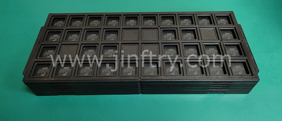
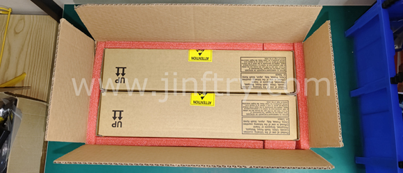
- Tray
-
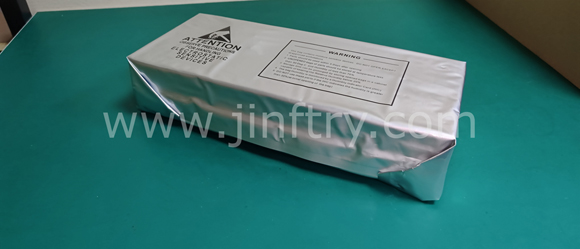
 Lead free / RoHS Compliant
 - 1977
- Запасы спот / разрешенные дилеры / излишки на заводе
- Гарантия качества на 1 год 》
- Нажмите, чтобы узнать цены
Службы доставки:

Способы оплаты:

| Part Number 5SGSMD8K3F40I3 |
| Category Embedded - FPGAs (Field Programmable Gate Array) |
| Manufacturer Altera |
| Description IC FPGA 696 I/O 1517FBGA |
| Package Tray |
| Series Stratix® V GS |
| Voltage - Supply 0.82V ~ 0.88V |
| Operating Temperature -40°C ~ 100°C (TJ) |
| Mounting Type Surface Mount |
| Package / Case 1517-BBGA, FCBGA |
| Supplier Device Package 1517-FBGA (40x40) |
| Number of I/O 696 |
| Number of Gates - |
| Number of LABs/CLBs 262400 |
| Number of Logic Elements/Cells 695000 |
| Total RAM Bits 51200000 |
| Package_case 1517-BBGA, FCBGA |
5SGSMD8K3F40I3 Гарантии


• Ответьте оперативно
• Гарантированное качество
• Глобальный доступ
• Конкурентоспособная рыночная цена
• Универсальные услуги цепочки поставок
Jinftry, это ваш самый надежный поставщик компонентов, добро пожаловать, чтобы отправить нам запрос, спасибо!
У вас есть вопросы о 5SGSMD8K3F40I3 ?
Не стесняйтесь связаться с нами:
+86-755-82518276
+8615019224070, annies65, +8615118125813
568248857, 827259012, 316249462
+8615019224070, +8615118118839, +8615118125813
( Электронная почта в первую очередь )
5SGSMD8K3F40I3 сопутствующие товары


Комментарии
Altera

5SGSED6N1F45C2N
IC FPGA 840 I/O 1932FBGA
5SGSED6N1F45C2LN
IC FPGA 840 I/O 1932FBGA
5SEEBH40C2N
IC FPGA 840 I/O 1932FBGA
5SEEBH40C2LN
IC FPGA 840 I/O 1932FBGA

5SEEBH40I3N
IC FPGA 840 I/O 1932FBGA

5SEEBH40I3LN
IC FPGA 840 I/O 1932FBGA

5SGXEBBR3H43C3N
IC FPGA 840 I/O 1932FBGA

5SGXEBBR3H43I4N
IC FPGA 840 I/O 1932FBGA
What is a data acquisition/data conversion IC?
What is a data acquisition/data conversion IC?
Data acquisition/data conversion ICs are a class of electronic integrated circuits used to collect and convert data. They play a key role in modern electronic systems, especially in the process of converting analog signals into digital signals.
The following is a detailed introduction to the data acquisition/data conversion IC:
Data acquisition and conversion principles
Data acquisition and conversion systems are used to acquire anal
74LS74 Double D Flip-Flop Characteristics Pin Data Sheet Application - Can Replace Introduction
74LS74 Pinout
74LS74 CAD Model
74LS74 Features
74LS74 Application
74LS74 Equivalent
What is 74LS74?
How to Use 74LS74
74LS74 Connection Diagram
74LS74 Package
74LS74 Manufacturer
Specifications
Parts with Similar Specs
How a programmable gate array (FPGA) works, its architecture, and how to program it
How a programmable gate array (FPGA) works, its architecture, and how to program it
Programmable Gate Array (FPGA, Field-Programmable Gate Array) is an integrated circuit that designers can program according to their needs after purchase. It includes a series of logic blocks and reconfigurable interconnections that allow designers to customize specific logic functions, data paths, or other specific circuit functions at the hardware level.
lm358 IC (amplifier circuit) datasheet, characteristics, pins, working principle, application fields and alternative models
lm358 IC (amplifier circuit) datasheet, characteristics, pins, working principle, application fields and alternative models
The LM358 IC is a very popular dual operational amplifier (Op-Amp). This model usually has different abbreviations such as lm386 ic, lm386 circuit, lm386 amplifier, lm386 amplifier circuit, etc.
The following is some basic information about it:
Manufacturer: Several companies make the LM358 op amp. It was originally designed by National Semiconductor, which was later