Altera 5SGSMD5K1F40I2

Изображение только для справки, пожалуйста, обратитесь к спецификации продукта
- 5SGSMD5K1F40I2
- Altera
- IC FPGA 696 I/O 1517FBGA
- Embedded - FPGAs (Field Programmable Gate Array)
- 5SGSMD5K1F40I2 Лист данных
- 1517-BBGA, FCBGA
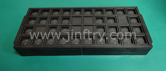
- Tray
-
 Lead free / RoHS Compliant
 - 28397
- Запасы спот / разрешенные дилеры / излишки на заводе
- Гарантия качества на 1 год 》
- Нажмите, чтобы узнать цены
Службы доставки:

Способы оплаты:

| Part Number 5SGSMD5K1F40I2 |
| Category Embedded - FPGAs (Field Programmable Gate Array) |
| Manufacturer Altera |
| Description IC FPGA 696 I/O 1517FBGA |
| Package Tray |
| Series Stratix® V GS |
| Voltage - Supply 0.87V ~ 0.93V |
| Operating Temperature -40°C ~ 100°C (TJ) |
| Mounting Type Surface Mount |
| Package / Case 1517-BBGA, FCBGA |
| Supplier Device Package 1517-FBGA (40x40) |
| Number of I/O 696 |
| Number of Gates - |
| Number of LABs/CLBs 172600 |
| Number of Logic Elements/Cells 457000 |
| Total RAM Bits 39936000 |
| Package_case 1517-BBGA, FCBGA |

5SGSMD5K1F40I2 Гарантии


• Ответьте оперативно
• Гарантированное качество
• Глобальный доступ
• Конкурентоспособная рыночная цена
• Универсальные услуги цепочки поставок
Jinftry, это ваш самый надежный поставщик компонентов, добро пожаловать, чтобы отправить нам запрос, спасибо!
У вас есть вопросы о 5SGSMD5K1F40I2 ?
Не стесняйтесь связаться с нами:
+86-755-82518276
+8615019224070, annies65, +8615118125813
568248857, 827259012, 316249462
+8615019224070, +8615118118839, +8615118125813
( Электронная почта в первую очередь )
5SGSMD5K1F40I2 сопутствующие товары


Комментарии
Altera

EP4SE530H35C2
IC FPGA 744 I/O 1152HBGA
10AX090U1F45I1SG
IC FPGA 744 I/O 1152HBGA
5SGXEA7N1F45I2N
IC FPGA 744 I/O 1152HBGA

10CL016YF484C8G
IC FPGA 744 I/O 1152HBGA

10CL016ZE144I8G
IC FPGA 744 I/O 1152HBGA

10M04SAU324I7G
IC FPGA 744 I/O 1152HBGA

10CL016YU484C8G
IC FPGA 744 I/O 1152HBGA

5SEEBH40I3L
IC FPGA 744 I/O 1152HBGA
Comparator performance and application and working principle
Comparators principle Comparators Performance indexComparators sort Zero-crossing voltage comparator: A typical amplitude comparison circuit, its circuit diagram and transmission characteristic curve are shown.
Voltage comparator: The voltage comparator is obtained by changing an input of the zero-crossing comparator from ground to a fixed voltage value.
What is a programmable logic IC?
What is a programmable logic IC?
A programmable logic device (PLD) is a special type of electronic component used in electronic systems. Unlike logic gates, which have fixed functionality, PLDs are manufactured with undefined functionality. They are highly flexible electronic components that can be programmed to be configured to perform a variety of logic functions.
Here's a closer look at some of the main types:
PLD (Programmable Logic Device): This is a basic form of programmable logic
Operational amplifier brief description, function, type and application field
Brief description of the operational amplifier:
An operational amplifier (Operational Amplifier, referred to as Op-Amp) is a DC-coupled high-gain electronic voltage amplifier whose output voltage is usually several hundred times the input differential voltage. Operational amplifiers usually incorporate power limiters, negative feedback networks, and gain controls, which are fundamental components in modern analog electronic circuits.
NVIDIA A100 80GB PCIe, A100 80GB SXM TENSOR CORE GPU is available in stock
Basic specifications of the NVIDIA A100 (these figures may vary by specific model and configuration):
GPU architecture: Ampere
Number of SMs: 108
Number of CUDA cores: 6912
Number of second-generation RT cores: 108
Number of third-generation Tensor cores: 432
Base Clock Frequency: 1410 MHz
Boost Clock Frequency: 1560 MHz
Memory size: 40GB or 80GB of HBM2
Memory bandwidth: 1555 GB/s (40GB version) or 2039 GB/s (80GB version)
Memory interface width: 5120 bits (40GB version) or 6144 bit