Altera 1SG210HN2F43E2VG

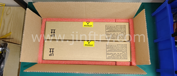
Изображение только для справки, пожалуйста, обратитесь к спецификации продукта
- 1SG210HN2F43E2VG
- Altera
- IC FPGA 688 I/O 1760FBGA
- Embedded - FPGAs (Field Programmable Gate Array)
- 1SG210HN2F43E2VG Лист данных
- 1760-BBGA, FCBGA
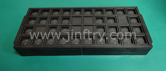
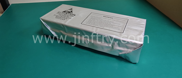
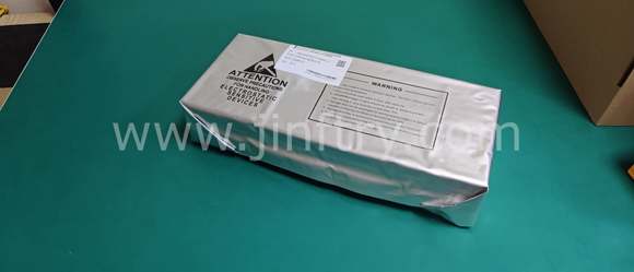
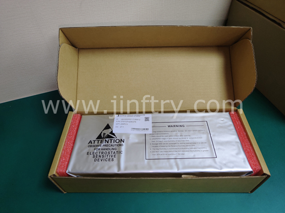
- Tray
-
 Lead free / RoHS Compliant
 - 3157
- Запасы спот / разрешенные дилеры / излишки на заводе
- Гарантия качества на 1 год 》
- Нажмите, чтобы узнать цены
Службы доставки:

Способы оплаты:

| Part Number 1SG210HN2F43E2VG |
| Category Embedded - FPGAs (Field Programmable Gate Array) |
| Manufacturer Altera |
| Description IC FPGA 688 I/O 1760FBGA |
| Package Tray |
| Series Stratix® 10 GX |
| Voltage - Supply 0.77V ~ 0.97V |
| Operating Temperature 0°C ~ 100°C (TJ) |
| Mounting Type Surface Mount |
| Package / Case 1760-BBGA, FCBGA |
| Supplier Device Package 1760-FBGA (42.5x42.5) |
| Number of I/O 688 |
| Number of Gates - |
| Number of LABs/CLBs 262500 |
| Number of Logic Elements/Cells 2100000 |
| Total RAM Bits - |
| Package_case 1760-BBGA, FCBGA |
1SG210HN2F43E2VG Гарантии


• Ответьте оперативно
• Гарантированное качество
• Глобальный доступ
• Конкурентоспособная рыночная цена
• Универсальные услуги цепочки поставок
Jinftry, это ваш самый надежный поставщик компонентов, добро пожаловать, чтобы отправить нам запрос, спасибо!
У вас есть вопросы о 1SG210HN2F43E2VG ?
Не стесняйтесь связаться с нами:
+86-755-82518276
+8615019224070, annies65, +8615118125813
568248857, 827259012, 316249462
+8615019224070, +8615118118839, +8615118125813
( Электронная почта в первую очередь )
1SG210HN2F43E2VG сопутствующие товары


Комментарии
Altera


1SG211HN2F43E2VG
IC FPGA 688 I/O 1760FBGA
1SG210HN2F43E2VGAS
IC FPGA 688 I/O 1760FBGA

1SG210HN3F43I2VG
IC FPGA 688 I/O 1760FBGA

1SG280HH3F55I3VG
IC FPGA 688 I/O 1760FBGA

1SG280HH3F55E2VG
IC FPGA 688 I/O 1760FBGA

1SG280HH3F55E2VGS3
IC FPGA 688 I/O 1760FBGA

1SG166HN3F43I2LG
IC FPGA 688 I/O 1760FBGA
1SG166HN2F43E2LG
IC FPGA 688 I/O 1760FBGA
battery charger
Battery charger according to the design circuit operating frequency to divide, can be divided into power frequency machine and high frequency machine. The power frequency machine is designed based on the traditional analog circuit principle, the internal power devices (such as transformers, inductors, capacitors, etc.) are larger, and there is generally less noise when the load is larger, but the model has strong resistance performance in the harsh grid environmental conditions, and the reliabil
What is the structure and function of PCB?
PCB (Printed Circuit Board) is one of the basic components in modern electronic equipment. It provides a platform to support and connect electronic components.
The internal structure of PCB is composed of multi-layer circuit board, conductive layer, insulating layer, pad, circuit layer, circuit spacing, circuit spacing, via holes, silk screen layer and solder mask layer. These components cooperate with each other to form a complete circuit board, providing reliable electrical connection and pro
The most complete introduction to 74LS32 Datasheet
The 74LS32 Datasheet contains important information about this integrated circuit such as detailed specifications, features, pin descriptions, electrical characteristics, operating conditions, absolute maximum ratings, and application information.
NVIDIA A100 80GB PCIe, A100 80GB SXM TENSOR CORE GPU is available in stock
Basic specifications of the NVIDIA A100 (these figures may vary by specific model and configuration):
GPU architecture: Ampere
Number of SMs: 108
Number of CUDA cores: 6912
Number of second-generation RT cores: 108
Number of third-generation Tensor cores: 432
Base Clock Frequency: 1410 MHz
Boost Clock Frequency: 1560 MHz
Memory size: 40GB or 80GB of HBM2
Memory bandwidth: 1555 GB/s (40GB version) or 2039 GB/s (80GB version)
Memory interface width: 5120 bits (40GB version) or 6144 bit